에피소드
IX: 이상한 명령어 LUI, AUIPC,
JAL, JALR 추가하기
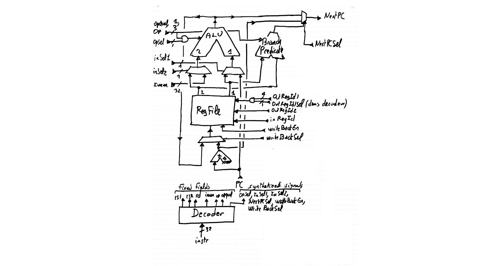
사실 이 명령어들은 그렇게 복잡하지 않습니다. 이 명령어들이 무엇을 해야 하는지 다시 살펴봅시다:
| 명령어 | 설명 | 알고리즘 |
|---|---|---|
LUI |
상위 즉시값 로드 | reg <- (im << 12) |
AUIPC |
PC에 상위 즉시값 더하기 | reg <- PC+(im << 12) |
JAL |
점프 후 링크 | reg <- PC+4 ; PC <- PC+imm |
JALR |
레지스터 기준 점프 후 링크 | reg <- PC+4 ; PC <- reg+imm |
먼저 대입문의 우변을 살펴봅시다. PC와 즉시값 사이의
덧셈을 계산해야 합니다. 이를 위한 ALU 입력용 mux 두 개가 이미 있으므로
따로 할 일은 없습니다. 다만 LUI는 즉시값을 레지스터에 바로
복사하므로 특별한 처리가 필요합니다. 이는 두 번째 레지스터의 선택
신호(sel2)를 디코더에서 나오는 추가 신호
regId1Sel과 AND 게이트로 묶으면 쉽게 처리할 수 있습니다. 이
신호가 0이면 해당 레지스터가 zero로 대체되어 즉시값에 0을
더하게 됩니다. 1비트 신호 하나를 추가하는 다소 우회적인 방법이지만, 이전
설계에 대한 변경을 최소화하고 / 복잡도도 최소한으로만 늘립니다. 이제
JAL과 JALR을 살펴봅시다. 이 두 명령어는
PC+4를 레지스터 파일에 다시 기록해야 합니다. 이를 위해
레지스터 파일의 라이트백(write back) 입력에 ALU 출력과 PC+4
중 하나를 선택하는 mux를 추가합니다. 이 두 가지 수정 사항은 위 회로도에
나와 있습니다.
이제 (거의 완성된) 명령어 디코더를 살펴볼 차례입니다. 복잡해
보이지만, 사실 7가지 명령어에 필요한 모든 신호를 생성하는 커다란
switch 문으로 작성된 큰 조합 함수에
불과합니다(load와 store는 아직 없으며, 다음
절에서 살펴보겠습니다). 명령어 디코더의 Verilog 소스를 보기 전에,
6502(80년대에 매우 널리 쓰인 8비트 프로세서)의 플로어 플랜(floor plan)을
살펴봅시다:
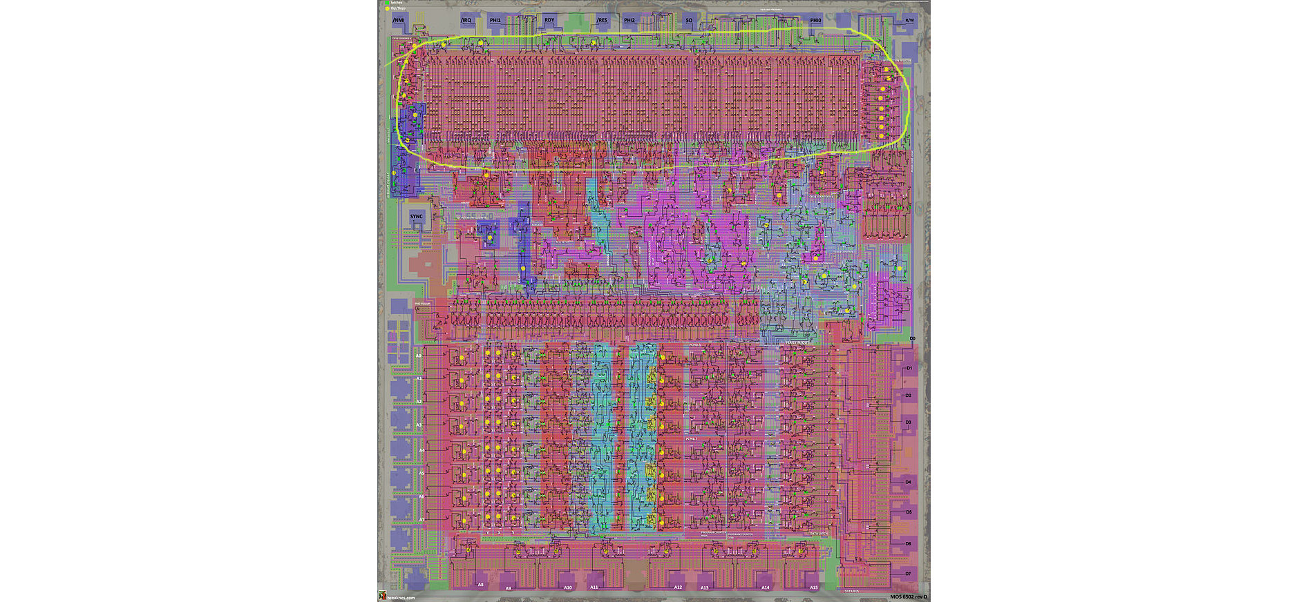
이 이미지는 위키백과에서 가져왔습니다. visual6502 프로젝트도
참고하십시오. 그곳에 많은 정보가 있습니다. 80년대 프로세서는 설계가
충분히 단순하므로 살펴볼 만합니다. 명령어 디코더는 이미지 상단에 있는
격자 모양의 구조입니다. 가로 방향으로는 현재 디코딩 중인 명령어의
8비트와 이를 반전한 8비트가 있고, 세로 방향으로는 이 비트들 사이에서
계산되는 모든 ANDs가 있으며(격자 위의 각 '점'이 하나의
AND에 해당합니다), 이 세로선들이 다시 ORs로
결합되어 프로세서의 내부 신호를 만듭니다.
다시 우리의 RISC-V 프로세서로 돌아갑시다. 둘보다 많은 소스 중 하나를 선택하는 신호는 소스마다 선을 하나씩 사용한다는 점에 유의하십시오(예를 들어 4개의 소스 중 하나를 선택할 때는 0001, 0010, 0100, 1000을 사용합니다). 이른바 원핫 인코딩(one hot encoding)이라 불리는 이 방식은 (00, 01, 10, 11)을 대신 쓸 수도 있으니 어리석어 보일 수 있지만, 실제로는 (당연히) 논리 깊이를 줄여 주고, 더 놀랍게도 결국 LUT를 절약하므로 이득만 있습니다.
module NrvDecoder(
    input wire [31:0] instr,
    output wire [4:0] writeBackRegId,
    output reg        writeBackEn,
    output reg [3:0]  writeBackSel, // 0001: ALU  0010: PC+4  (and also, later, 0100:RAM 1000:counters)
    output wire [4:0] inRegId1,
    output wire [4:0] inRegId2,
    output reg        aluSel, // 0: force aluOp,aluQual to zero (ADD)  1: use aluOp,aluQual from instr field
    output reg        aluInSel1, // 0: reg  1: pc
    output reg        aluInSel2, // 0: reg  1: imm
    output [2:0]      aluOp,
    output reg        aluQual,
    output reg [2:0]  nextPCSel, // 001: PC+4  010: ALU  100: (predicate ? ALU : PC+4)
    output reg [31:0] imm,
    output reg        error
);

   reg inRegId1Sel; // 0: force inRegId1 to zero 1: use inRegId1 instr field

   // The control signals directly deduced from (fixed pos) fields
   assign writeBackRegId = instr[11:7];
   assign inRegId1       = instr[19:15] & {5{inRegId1Sel}}; // Internal sig InRegId1Sel used to force zero in reg1
   assign inRegId2       = instr[24:20];
   assign aluOp          = instr[14:12];

   // The five immediate formats, see the RiscV reference, Fig. 2.4 p. 12
   wire [31:0] Iimm = {{21{instr[31]}}, instr[30:20]};
   wire [31:0] Simm = {{21{instr[31]}}, instr[30:25], instr[11:7]};
   wire [31:0] Bimm = {{20{instr[31]}}, instr[7], instr[30:25], instr[11:8], 1'b0};
   wire [31:0] Jimm = {{12{instr[31]}}, instr[19:12], instr[20], instr[30:21], 1'b0};
   wire [31:0] Uimm = {instr[31], instr[30:12], {12{1'b0}}};

   // The rest of instruction decoding, for the following signals:
   // writeBackEn
   // writeBackSel   0001: ALU  0010: PC+4 (two additional bits for RAM and COUNTERS)
   // inRegId1Sel    0: zero   1: regId
   // aluInSel1      0: reg    1: PC
   // aluInSel2      0: reg    1: imm
   // aluQual        +/- SRLI/SRAI
   // aluSel         0: force aluOp,aluQual=00  1: use aluOp/aluQual
   // nextPCSel      001: PC+4  010: ALU   100: (pred ? ALU : PC+4)
   // imm (select one of Iimm,Simm,Bimm,Jimm,Uimm)

   // We need to distingish shifts, because
   //   for ALU ops with immediates, aluQual is 0, except
   //   for shifts (then it is instr[30]). Had a hard time
   //   debugging / understanding that.
   wire aluOpIsShift = (aluOp == 3'b001) || (aluOp == 3'b101);

   always @(*) begin

       error = 1'b0;
       nextPCSel = 3'b001;  // default: PC <- PC+4
       inRegId1Sel = 1'b1; // reg 1 Id from instr
       aluQual = 1'b0;

       (* parallel_case, full_case *)
       case(instr[6:0])
       7'b0110111: begin // LUI
          writeBackEn  = 1'b1;    // enable write back
          writeBackSel = 4'b0001; // write back source = ALU
          inRegId1Sel = 1'b0;     // reg 1 Id = 0
          aluInSel1 = 1'b0;       // ALU source 1 = reg
          aluInSel2 = 1'b1;       // ALU source 2 = imm
          aluSel = 1'b0;          // ALU op = ADD
          imm = Uimm;             // imm format = U
       end

       7'b0010111: begin // AUIPC
          writeBackEn  = 1'b1;    // enable write back
          writeBackSel = 4'b0001; // write back source = ALU
          inRegId1Sel = 1'bx;     // reg 1 Id : don't care (we use PC)
          aluInSel1 = 1'b1;       // ALU source 1 = PC
          aluInSel2 = 1'b1;       // ALU source 2 = imm
          aluSel = 1'b0;          // ALU op = ADD
          imm = Uimm;             // imm format = U
       end

       7'b1101111: begin // JAL
          writeBackEn  = 1'b1;    // enable write back
          writeBackSel = 4'b0010; // write back source = PC+4
          inRegId1Sel = 1'bx;     // reg 1 Id : don't care (we use PC)
          aluInSel1 = 1'b1;       // ALU source 1 = PC
          aluInSel2 = 1'b1;       // ALU source 2 = imm
          aluSel = 1'b0;          // ALU op = ADD
          nextPCSel = 3'b010;     // PC <- ALU
          imm = Jimm;             // imm format = J
       end

       7'b1100111: begin // JALR
          writeBackEn  = 1'b1;    // enable write back
          writeBackSel = 4'b0010; // write back source = PC+4
          aluInSel1 = 1'b0;       // ALU source 1 = reg
          aluInSel2 = 1'b1;       // ALU source 2 = imm
          aluSel = 1'b0;          // ALU op = ADD
          nextPCSel = 3'b010;     // PC <- ALU
          imm = Iimm;             // imm format = I
       end

       7'b1100011: begin // Branch
          writeBackEn = 1'b0;     // disable write back
          writeBackSel = 4'bxxxx; // write back source = don't care
          aluInSel1 = 1'b1;       // ALU source 1 : PC
          aluInSel2 = 1'b1;       // ALU source 2 : imm
          aluSel = 1'b0;          // ALU op = ADD
          nextPCSel = 3'b100;     // PC <- pred ? ALU : PC+4
          imm = Bimm;             // imm format = B
       end

       7'b0010011: begin // ALU operation: Register,Immediate
          writeBackEn = 1'b1;     // enable write back
          writeBackSel = 4'b0001; // write back source = ALU
          aluInSel1 = 1'b0;       // ALU source 1 : reg
          aluInSel2 = 1'b1;       // ALU source 2 : imm
                                  // Qualifier for ALU op: SRLI/SRAI
          aluQual = aluOpIsShift ? instr[30] : 1'b0;
          aluSel = 1'b1;         // ALU op : from instr
          imm = Iimm;            // imm format = I
       end

       7'b0110011: begin // ALU operation: Register,Register
          writeBackEn = 1'b1;     // enable write back
          writeBackSel = 4'b0001; // write back source = ALU
          aluInSel1 = 1'b0;       // ALU source 1 : reg
          aluInSel2 = 1'b0;       // ALU source 2 : reg
          aluQual = instr[30];    // Qualifier for ALU op: +/- SRL/SRA
          aluSel = 1'b1;          // ALU op : from instr
          error = instr[25];
          imm = 32'bxxxxxxxxxxxxxxxxxxxxxxxxxxxxxxxx; // don't care
       end

           default: begin
          writeBackEn = 1'b0;
          error = 1'b1;
          writeBackSel = 4'bxxxx;
          inRegId1Sel = 1'bx;
          aluInSel1 = 1'bx;
          aluInSel2 = 1'bx;
          aluSel = 1'bx;
          nextPCSel = 3'bxxx;
          imm = 32'bxxxxxxxxxxxxxxxxxxxxxxxxxxxxxxxx;
       end
       endcase
   end

endmodule